

Imagine a world where digital information doesn’t just live on a screen but is seamlessly woven into the very fabric of your physical reality, accessible with a simple glance. This is the promise of augmented reality glasses, a technology poised to redefine human-computer interaction. The journey from this tantalizing vision to a comfortable, functional, and affordable device on your face is one of the most formidable engineering challenges of our time. It’s a story not just of software and code, but of precision optics, advanced materials, and manufacturing ingenuity on a microscopic scale. The race to perfect this technology is not merely a competition between corporations; it is a collective push to build the next fundamental platform for how we work, learn, and connect.
The Core Architectural Challenge: Merging the Digital and Physical
At its heart, the manufacturing of augmented reality glasses is an exercise in contradiction. The device must be powerful enough to run complex spatial computing algorithms, yet small and light enough to be worn all day. It must project bright, high-resolution images that are visible in broad daylight, but consume so little power that the battery isn't drained in an hour. It must contain a suite of sensors to understand the world, yet remain socially acceptable and aesthetically pleasing. Balancing these competing demands is the central puzzle that defines the entire manufacturing process.
Through the Looking Glass: The Optics and Display Systems
The most critical component, and the one that dictates the entire form factor, is the optical system. This is the engine that generates the digital light and directs it into the user’s eye. Unlike a projector that throws an image onto a wall, these optics must superimpose a stable image onto the user’s real-world view, a task requiring incredible precision.
Waveguide Technology: The Leading Contender
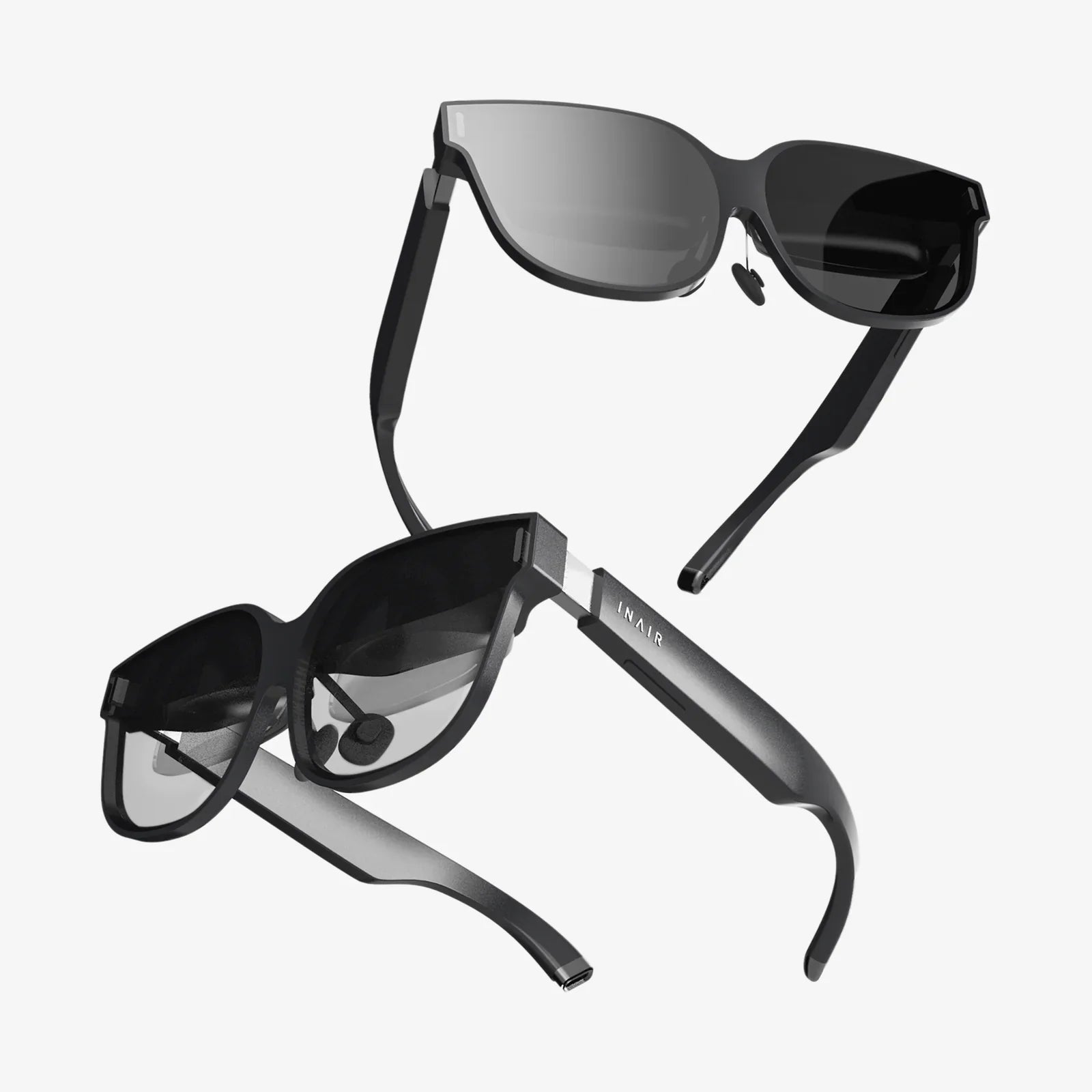
The most promising path for consumer-grade devices is the waveguide. Think of a waveguide as a flat, transparent piece of glass or plastic that acts like a conduit for light. The process begins with a micro-display, a tiny screen that generates the initial image. This light is then coupled into the edge of the waveguide using miniature gratings or lenses. Once inside, the light travels through the substrate via total internal reflection—bouncing from surface to surface like a whisper in a hallway.
At specific points, out-coupling structures, often microscopic diffractive optical elements (DOEs) or holographic films, bend a portion of this light out of the waveguide and directly into the user’s eye. The complexity of manufacturing these waveguides is immense. They are typically made using semiconductor-like processes such as nanoimprint lithography, where a master mold with nanoscale features is pressed into a resin-coated substrate, which is then cured with UV light. The alignment tolerances are less than a micron, requiring a cleanroom environment and equipment of the highest precision. Any defect, no matter how small, results in visual artifacts like ghosting, blur, or a noticeable rainbow effect.
Alternative Optical Architectures
While waveguides are the focus for sleek, glasses-like designs, other methods are used, particularly in bulkier industrial or enterprise-focused models. Birdbath optics use a beamsplitter—a partially mirrored surface—to reflect light from a micro-OLED display into the eye, combining it with the view of the real world seen through the combiner lens. This can offer brilliant colors and high contrast but often results in a smaller field of view and a boxier design. Curved mirror designs, or freeform optics, use complex, non-symmetrically curved surfaces to fold the optical path and magnify the image. These can be highly efficient but are challenging to mass-produce with consistency. The choice of optical system is a fundamental trade-off between field of view, image quality, form factor, and, most importantly, manufacturability and cost.
The Hardware Ecosystem: Sensors, Processors, and Power
A pair of advanced augmented reality glasses is essentially a wearable supercomputer. Its purpose is to understand the environment and anchor digital content within it, a task that requires a sophisticated array of hardware.
Environmental Understanding
To seamlessly blend digital and physical, the device must perceive the world in three dimensions. This is achieved through a suite of sensors typically including:
- Cameras: Multiple cameras serve different purposes. Standard RGB cameras capture the color view of the world. Depth-sensing cameras, using technologies like structured light or time-of-flight (ToF), fire out patterns of infrared light and measure their deformation or return time to create a real-time 3D map of the environment. This is crucial for occlusion (having digital objects hide behind real-world furniture) and for understanding surfaces.
- Inertial Measurement Units (IMUs): These accelerometers and gyroscopes track the precise movement and rotation of the user’s head with extremely low latency, preventing the image from lagging behind and causing motion sickness.
- Eye-Tracking Cameras: By projecting infrared light onto the user’s eyes and analyzing the reflection, these internal cameras determine exactly where the user is looking. This is vital for creating a natural depth of field, enabling intuitive interface interaction through gaze, and enabling foveated rendering—a power-saving technique where the highest resolution is only rendered in the center of the gaze.
The Onboard Brain and Its Limitations
Processing the torrent of data from these sensors is a monumental task. It involves simultaneous localization and mapping (SLAM) to create a persistent map of the space, hand-tracking algorithms, object recognition, and rendering complex 3D graphics. Much of this processing is handled by a dedicated system-on-a-chip (SoC) designed for extreme efficiency. Thermal management becomes a critical constraint; these powerful chips generate heat in a device with no space for a fan. Engineers must use advanced heat sinks and strategically place components to dissipate warmth away from the user’s face, often relying on the device's frame itself as a heatsink.
The Power Dilemma
All this technology is incredibly power-hungry. The brightest displays drain batteries fastest. This leads to another tough compromise: battery life versus weight. Large batteries are heavy and uncomfortable on the head. Therefore, much of the manufacturing innovation is focused on extreme power efficiency—in the displays, the processors, and the software. Some designs opt for a wired connection to a battery pack in the user’s pocket, while others strive for all-day battery life within the glasses frame itself, a goal that pushes the limits of current battery energy density.
Materials and Ergonomics: The Human Factor
A technological marvel is useless if people won’t wear it. This makes industrial design and material science as important as optical engineering.
Lightweighting and Durability
The quest for lightness leads manufacturers to advanced materials. Titanium is often used for its superior strength-to-weight ratio in critical hinges and frames. High-grade polymers and composite materials, sometimes with carbon fiber reinforcement, form the main body of the frames. These materials must be durable enough to withstand daily wear and tear, yet flexible enough for a comfortable fit. The lenses themselves, whether prescription or plano, are coated with anti-reflective, anti-scratch, and often anti-smudge coatings applied through physical vapor deposition processes.
The Customization Imperative
Unlike a one-size-fits-all smartphone, glasses are deeply personal. They must accommodate a vast range of head shapes, nose bridge sizes, and, critically, vision corrections. Manufacturing must therefore accommodate custom prescription lenses that are digitally aligned and bonded to the waveguide assembly. This requires a flexible manufacturing line that can handle mass customization, where each unit can be slightly different. Interchangeable nose pads and adjustable temples are not afterthoughts; they are essential components that require their own precise tooling and assembly processes.
The Assembly Process: A Dance of Precision
Bringing all these components together is an exercise in microscopic precision, often described as "watchmaking at scale." Automated assembly lines, frequently assisted by robotic arms and computer vision systems, are the norm.
The process often begins with the precise placement of the micro-display and its alignment to the in-coupling grating on the waveguide. This alignment, often done with active optical feedback, is perhaps the single most critical step in the entire process. A misalignment of even a few microns will ruin the image quality. Next, the waveguide is carefully seated into the frame, which itself has been injection-molded or machined. The sensor array is then installed, with each camera and IMU requiring precise calibration against known targets to ensure their data aligns perfectly with the optical view.
Finally, the software is loaded and the device undergoes a rigorous battery of quality assurance tests. These tests check for optical performance (brightness, uniformity, contrast), sensor accuracy, wireless connectivity, and battery performance. Each unit is not just assembled; it is individually calibrated and validated. This level of attention makes the manufacturing process far more akin to producing high-end scientific instruments than consumer electronics.
The Future of Manufacturing: Scaling the Summit
The current state of manufacturing is capable of producing incredible devices, but primarily at high costs and relatively low volumes. The next great challenge is scaling this precision to the hundreds of millions of units required for true mass-market adoption. This will require breakthroughs in several areas. New, more forgiving optical materials could simplify waveguide production. Higher-yield manufacturing processes for nanoimprint lithography will drive down the cost of the most expensive component. advancements in heterogeneous integration could allow sensors and processors to be packaged together more tightly and efficiently, saving space and power. The ultimate goal is a virtuous cycle: better manufacturing yields lead to lower costs, which leads to wider adoption, which fuels investment in even more advanced manufacturing techniques.
The factory that successfully masters the high-volume, high-precision, and customizable assembly of augmented reality glasses will not just be building a product; it will be building the windows through which humanity will increasingly experience a blended world of bits and atoms. The stakes, and the potential rewards, could not be higher.
We stand on the precipice of a new era, one where the line between our digital and physical lives will finally dissolve. The sleek pair of glasses resting on your nose will become a portal, a tireless assistant, and a canvas for creativity, all enabled by a manufacturing process that is quietly achieving the near-impossible. The journey from the laboratory cleanroom to your living room is a testament to human ingenuity, and it’s a journey that is just beginning. The future isn't just something we will see on a screen; we will live inside it, and it will all start with a look.
Share:
Best Augmented Reality Glasses 2025 Comparison: A Deep Dive into the Future on Your Face
Virtual Reality Glasses: A Portal to New Realities and the Future of Human Experience